- 您现在的位置:买卖IC网 > Sheet目录342 > MCBSTM32EXL (Keil)BOARD EVALUATION FOR STM32F103ZE
�� �
�
�Analog-to-digital� converter� (ADC)�
�Example:�
�n� =� 1,� channels� to� be� converted� =� 1,� 2,� 3�
�1st� trigger:� channel� 1� converted�
�2nd� trigger:� channel� 2� converted�
�3rd� trigger:� channel� 3� converted� and� EOC� and� JEOC� events� generated�
�4th� trigger:� channel� 1�
�RM0008�
�Note:�
�11.4�
�Note:�
�11.5�
�206/995�
�1�
�2�
�3�
�1�
�2�
�When� all� injected� channels� are� converted,� the� next� trigger� starts� the� conversion� of� the� first�
�injected� channel.� In� the� example� above,� the� 4th� trigger� reconverts� the� 1st� injected� channel�
�1.�
�It� is� not� possible� to� use� both� auto-injected� and� discontinuous� modes� simultaneously.�
�The� user� must� avoid� setting� discontinuous� mode� for� both� regular� and� injected� groups�
�together.� Discontinuous� mode� must� be� enabled� only� for� one� group� conversion.�
�Calibration�
�The� ADC� has� an� built-in� self� calibration� mode.� Calibration� significantly� reduces� accuracy�
�errors� due� to� internal� capacitor� bank� variations.� During� calibration,� an� error-correction� code�
�(digital� word)� is� calculated� for� each� capacitor,� and� during� all� subsequent� conversions,� the�
�error� contribution� of� each� capacitor� is� removed� using� this� code.�
�Calibration� is� started� by� setting� the� CAL� bit� in� the� ADC_CR2� register.� Once� calibration� is�
�over,� the� CAL� bit� is� reset� by� hardware� and� normal� conversion� can� be� performed.� It� is�
�recommended� to� calibrate� the� ADC� once� at� power-on.� The� calibration� codes� are� stored� in�
�the� ADC_DR� as� soon� as� the� calibration� phase� ends.�
�It� is� recommended� to� perform� a� calibration� after� each� power-up.�
�Before� starting� a� calibration� the� ADC� must� have� been� in� power-off� state� (ADON� bit� =� ‘0’)� for�
�at� least� two� ADC� clock� cycles.�
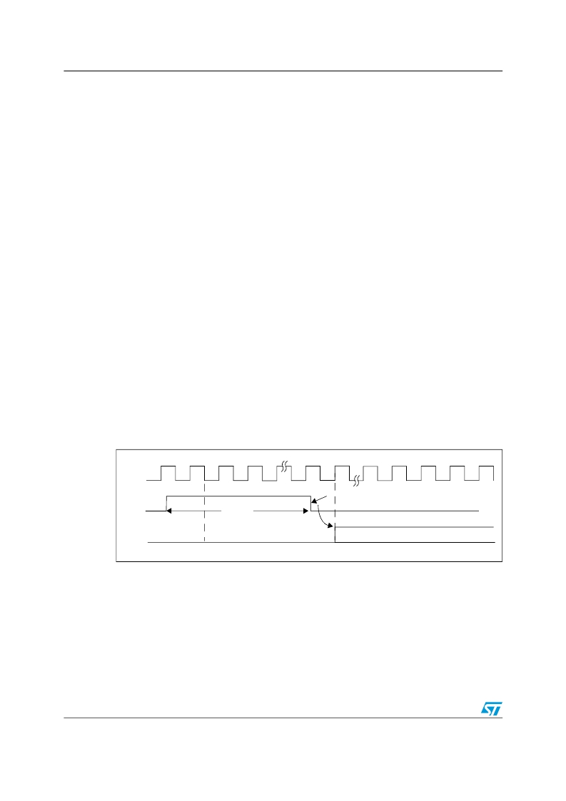
�Figure� 29.� Calibration� timing� diagram�
�CLK�
�Calibration� Reset� by� Hardware�
�Calibration� ongoing�
�CAL�
�t� CAL�
�Normal� ADC� Conversion�
�ADC�
�Conversion�
�Data� alignment�
�ALIGN� bit� in� the� ADC_CR2� register� selects� the� alignment� of� data� stored� after� conversion.�
��The� injected� group� channels� converted� data� value� is� decreased� by� the� user-defined� offset�
�written� in� the� ADC_JOFRx� registers� so� the� result� can� be� a� negative� value.� The� SEXT� bit� is�
�the� extended� sign� value.�
�For� regular� group� channels� no� offset� is� subtracted� so� only� twelve� bits� are� significant.�
�Doc� ID� 13902� Rev� 9�
�发布紧急采购,3分钟左右您将得到回复。
相关PDF资料
MCBTMPM330
BOARD EVAL TOSHIBA TMPM330 SER
MCIMX25WPDKJ
KIT DEVELOPMENT WINCE IMX25
MCIMX53-START-R
KIT DEVELOPMENT I.MX53
MCM69C432TQ20
IC CAM 1MB 50MHZ 100LQFP
MCP1401T-E/OT
IC MOSFET DRVR INV 500MA SOT23-5
MCP1403T-E/MF
IC MOSFET DRIVER 4.5A DUAL 8DFN
MCP1406-E/SN
IC MOSFET DVR 6A 8SOIC
MCP14628T-E/MF
IC MOSFET DVR 2A SYNC BUCK 8-DFN
相关代理商/技术参数
MCBSTM32EXLU
功能描述:开发板和工具包 - ARM EVAL BOARD + ULINK2 FOR STM32F103ZG
RoHS:否 制造商:Arduino 产品:Development Boards 工具用于评估:ATSAM3X8EA-AU 核心:ARM Cortex M3 接口类型:DAC, ICSP, JTAG, UART, USB 工作电源电压:3.3 V
MCBSTM32EXLU-ED
制造商:ARM Ltd 功能描述:KEIL STM STM32EXL EVAL BOARD
MCBSTM32EXLUME
功能描述:开发板和工具包 - ARM EVAL BOARD + ULINKME FOR STM32F103ZG
RoHS:否 制造商:Arduino 产品:Development Boards 工具用于评估:ATSAM3X8EA-AU 核心:ARM Cortex M3 接口类型:DAC, ICSP, JTAG, UART, USB 工作电源电压:3.3 V
MCBSTM32F200
功能描述:开发板和工具包 - ARM EVAL BOARD FOR STM STM32F207IG
RoHS:否 制造商:Arduino 产品:Development Boards 工具用于评估:ATSAM3X8EA-AU 核心:ARM Cortex M3 接口类型:DAC, ICSP, JTAG, UART, USB 工作电源电压:3.3 V
MCBSTM32F200U
功能描述:开发板和工具包 - ARM EVAL BOARD FOR STM STM32F207IG + ULINK2
RoHS:否 制造商:Arduino 产品:Development Boards 工具用于评估:ATSAM3X8EA-AU 核心:ARM Cortex M3 接口类型:DAC, ICSP, JTAG, UART, USB 工作电源电压:3.3 V
MCBSTM32F200UME
功能描述:开发板和工具包 - ARM EVAL BOARD FOR STM STM32F207IG ULINK-ME
RoHS:否 制造商:Arduino 产品:Development Boards 工具用于评估:ATSAM3X8EA-AU 核心:ARM Cortex M3 接口类型:DAC, ICSP, JTAG, UART, USB 工作电源电压:3.3 V
MCBSTM32F200UME-ED
制造商:ARM Ltd 功能描述:KEIL STM32F207IG EVAL BOARD
MCBSTM32F400
功能描述:开发板和工具包 - ARM EVAL BOARD FOR STM STM32F407IG
RoHS:否 制造商:Arduino 产品:Development Boards 工具用于评估:ATSAM3X8EA-AU 核心:ARM Cortex M3 接口类型:DAC, ICSP, JTAG, UART, USB 工作电源电压:3.3 V